| View previous topic :: View next topic |
| Author |
Message |
ckl
Joined: 14 Jan 2016
Posts: 105
|
 Posted: Thu Jan 14, 2016 1:18 pm Post subject: How to get started? Posted: Thu Jan 14, 2016 1:18 pm Post subject: How to get started? |
 |
|
Hello.
I introduced myself in the off topic section because I wasn't sure where to post an intro and my question. Somebody suggested that I post here to get a quicker answer.
So basically, I was cleaning out my garage and found a bunch of old motherboards with the CPU still attached in my pile of computer junk. I decided to take the CPU's out and keep them. When I was researching them on the internet, I found this site and the beautiful die shots that everyone is posting. That led me to wonder how one is able to take apart the CPU to get to the die and photograph it. So I went and googled that, but came up with limited results. The results are mostly about taking off the IHS for cooling purposes. I also found some videos on using harsh chemicals to dissolve the packaging to expose the die. It seems that a lot of the die shots posted here are so perfect that it doesn't seem like harsh chemicals were used to expose them.
Anyway, I also learned that modern chips are packaged in such a way as to make it near impossible for weekend hobbyists like myself to deconstruct to expose the die. But what year did this happen? Is it pre-2000's?
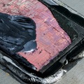
Of the CPU's that I have, a lot of them are packaged differently. And there aren't many helpful tips anywhere as to how to take them apart if it is even possible to do it. So, here are the pics of the CPU's both top and bottom and if any of the experts would kindly give me any tips on whether I should do it and what process I should apply in exposing the die.
Thanks for reading.
PS: You can click the pics to go to the website and click the magnifying glass to get the full resolution picture.


Last edited by ckl on Thu Nov 02, 2017 3:32 pm; edited 1 time in total |
|
| Back to top |
|
 |
Birdman.

Joined: 13 Nov 2012
Posts: 833
Location: Finland
|
| Posted: Thu Jan 14, 2016 2:57 pm Post subject: |
|
|
Hello and welcome to this forum!
Unfortunately, all CPUs in your pic are difficult ones for die shots. All others are modern flipchip ones indeed except black Mendocino Celeron that has the interesting side of die covered by black epoxy with markings.
To take nice pics of flip-chip dies you'll have to desolder the die by heating and then clean underfill and C4 solder balls to see top metal layer of the die. That cleaning is already difficult and usually top metal layer of those dies doesn't look so interesting, so for nice pic you'll also have to delayer the die using acid or lapping/polishing. So far the only one taking die shots of flipchip CPUs successfully at https://www.flickr.com/photos/130561288@N04/ doesn't seem to be a member of this forum yet.
Mendocino Celeron requires similar tricks to open as plastic chips. There you'll need very strong or preferably fuming acid to dissolve plastic or epoxy. Other option is to try burning the package with gas torch so that it breaks and gives you separate die if you're lucky. Anyway, both methods are dangerous and release toxic fumes, so you'll need proper fume hood.
However, many CPUs from 4004 to Pentium 1 era are wirebond chips in ceramic packages, or in many cases such version exists in addition to plastic version. Those are the easy ones, and most of my die shots at this forum and at https://commons.wikimedia.org/wiki/User:Birdman86 are taken of wirebond chips in ceramic packages (except some plastic ones burnt open by forum member aberco or found as separate unpackaged dies or wafers).
Wirebond chips in ceramic packages have some lid or plate covering the die, and all you'll have to do before taking nice die shots is to remove that lid. Lid may be metal plate soldered on ceramic package, and in that case you can desolder it by carefully pushing knife or flat sharpened screwdriver under it while heating with heat gun. Just be careful that your tool doesn't get into the die cavity and scratch the die or then slip back out from under the lid so that lid can shoot melted solder on the die.
Lid may also be caramic plate glued by epoxy or something else, and in that case I've shock cooled the lid with water to crack glue or lid if glue doesn't melt while heating with heat gun. Some packages (like Intel D-type and Motorola FE-type) have two ceramic plates glued together, and in that case I've also used shock cooling with water if heating and forcing with screwdriver doesn't separate the plates. Heating quickly with gas torch also works as alternative to shock cooling with water, but there the lid may fly off fast due to high pressure in die cavity or you may damage the die if flame hits it too long after lid has flown off.
You can also check http://www.cpu-world.com/forum/viewtopic.php?t=19888 where I've collected die shots taken by others. Luckily, CPU manufacturers usually release nice die shots also when they release new CPUs, so you'll find die shots of all Core i7 generations there and many other later CPUs also. I just updated that thread to fix broken links and add latest CPUs there. |
|
| Back to top |
|
|
ckl
Joined: 14 Jan 2016
Posts: 105
|
| Posted: Thu Jan 14, 2016 4:51 pm Post subject: |
|
|
Thanks for the explanation!
I've been looking at your die shots and they are awesome! My reason for taking CPU's apart is not just for photography, but for allowing my kids to look at them through a microscope as well. It's just not quite the same looking at an image vs. handling the actual chip and looking at it through a high powered lens at various magnification.
What peaked their interest was when I dug up a couple of silicon wafers, one that was some sort of controller chip and the other some sort of RAM, and showed it to them under a magnifying glass and then under a microscope at 300x. They were utterly amazed... including myself since this is the first time I looked at it under such magnification. These wafers were gifted to me from a friend who worked at TSMC a decade a ago when I visited him in Taiwan... at the time, I was a clueless idiot and didn't truly appreciate the technology behind the manufacture of these wafers. Now, I'm just a little less clueless I suppose.
So now I want to show them something that is more complex so that is how I ended up rummaging these CPU's out of the garage. But I guess it will take a lot of time and effort to do this so I might as well just go buy some wafers or wirebonded CPU's from the "for sale" forum and make my life easier. I may decide to decap one of the Pentium 4's and then sand it down to see if I can do it. That would be a good showpiece to have somebody look at the cpu with the heat spreader on it, then be able to remove it and see the actual CPU die underneath (like in the photos of the link in your post).
I'm not sure how that person was able to get the cpu die exposed on his CPU. It seems like he's got a flipchip, but then just sanded from the "uninteresting side" to get down to the "interesting side?" without ever taking the die off the package. Is that possible? Or did he take the die off the package, sanded the "interesting side" to expose the die, then glued it back onto the package with the "interesting side" up?
Anyway, if I'm successful, I'll post some of the photos. I'll also post some photos of those wafers so somebody can tell me what they actually are. |
|
| Back to top |
|
|
Birdman.
Joined: 13 Nov 2012
Posts: 833
Location: Finland
|
| Posted: Thu Jan 14, 2016 6:31 pm Post subject: |
|
|
He has desoldered the dies from packages, sanded the interesting solder/underfill side until nice details are visible and then glued the silicon side of die back on package with interesting side up. He has thus flipped the dies to show interesting details of die on package and sanded most or all metal layers away leaving silicon there and some lower layers on it.
It's likely not possible to sand all the silicon away because that's thick layer of hard silicon with soft and very thin interesting layers under it. My friend has tried to dissolve silicon with KOH, but that seems to work OK only for 130 nm AMD CPUs. That's how I got my Thoroughbred and Barton pics when thin film with metal layers detached after silicon, solder and underfill dissolved in almost boiling saturated KOH solution. |
|
| Back to top |
|
|
ckl
Joined: 14 Jan 2016
Posts: 105
|
| Posted: Thu Jan 14, 2016 6:42 pm Post subject: |
|
|
So if I understand you correctly, if I just take the IHS off to expose the "uninteresting side" of the die, and then started sanding that side, it wouldn't work because a) the material is too hard b) when I get down to the "interesting side" it will be too brittle or soft?
If that's not recommended (to start from the uninteresting side), can i use a heat gun to separate the die from the package? I don't quite understand how he separated the die from the package without destroying the package.
Last edited by ckl on Thu Jan 14, 2016 7:41 pm; edited 2 times in total |
|
| Back to top |
|
|
Birdman.
Joined: 13 Nov 2012
Posts: 833
Location: Finland
|
| Posted: Thu Jan 14, 2016 7:24 pm Post subject: |
|
|
Yes, you can use heat gun to separate die from package. Heat melts solder balls and makes underfill brittle. Thus, you can take out that brittle underfill from one corner or side with some blade until you get your blade under die to carefully lift it, or possibly underfill just cracks when solder melts so that die detaches and starts moving. It's also possible that die sticks to heatspreader if you heat it enough with heat gun before attempting to remove heatspreader, but that should be nice because it's easier to handle the die on heatspreader. Anyway, separating flip-chip dies from packages shouldn't be too difficult, at least my first attempt with UltraSPARC II was successful.
Sanding the silicon away that holds the die together just isn't a good idea because that leaves too thin and soft layers on non-uniform solder balls and underfill. It's also too much work if you don't want to be too quick so that everything interesting just disappears before you notice it. Sanding underfill, solder balls and thin metal layers away should be quite easy and leaves silicon there to hold the die together. However, it's likely very difficult to get fine enough result without scratches and with as much sanding everywhere with the same layer visible. |
|
| Back to top |
|
|
ckl
Joined: 14 Jan 2016
Posts: 105
|
| Posted: Thu Jan 14, 2016 7:42 pm Post subject: |
|
|
| Birdman. wrote: | Yes, you can use heat gun to separate die from package. Heat melts solder balls and makes underfill brittle. Thus, you can take out that brittle underfill from one corner or side with some blade until you get your blade under die to carefully lift it, or possibly underfill just cracks when solder melts so that die detaches and starts moving. It's also possible that die sticks to heatspreader if you heat it enough with heat gun before attempting to remove heatspreader, but that should be nice because it's easier to handle the die on heatspreader. Anyway, separating flip-chip dies from packages shouldn't be too difficult, at least my first attempt with UltraSPARC II was successful.
|
Thanks for taking the time to teach me all this stuff. I'm getting excited!
I'm also now confused. I read your comments on the Mondecino Celeron and found that it is a Plastic PGA vs. FCPGA. So I researched that and found this definition:
"PPGA (plastic pin grid array) is a microchip design from Intel that has the silicon core of the microchip facing down toward the computer motherboard"
"Intel has also developed another chip design called FC-PGA ( flip chip-pin grid array ). FC-PGA packages have the processor core flipped up on the back of the chip, facing away from the motherboard"
From those definitions, the interesting side of the die in a PPGA is opposite that of the FCPGA. So all flipchip designs have the interesting side facing down towards the motherboard. So in the PPGA, the interesting side is facing up?
If that's the case, then to expose the interesting side of the Mendocino, I would have to desolder the metal portion... not dissolve the plastic? Which is opposite of what you said.
Any comments?
Sorry for my lame terminology (ie. interesting side). I'm still wrapping my head around the various terms (decapping, delidding, PGA, PPGA, FCPGA, BGA, etc). |
|
| Back to top |
|
|
Birdman.
Joined: 13 Nov 2012
Posts: 833
Location: Finland
|
| Posted: Thu Jan 14, 2016 8:12 pm Post subject: |
|
|
I've actually desoldered top metal plate of Pentium MMX in PPGA package and that shows the wrong side of die indeed. Mendocino is still wirebond chip with wires in black epoxy attached to the interesting side of the die. There just can't be wiring on the top of the chip with that metal heatspreader.
All common Intel CPUs in CPGA, PPGA and FCPGA packages have interesting side of die towards motherboard, there's just air touching that interesting side of die in old CPGA, epoxy in PPGA and underfill in FCPGA in addition to wiring/solder balls. However, some CPGA (like 68020) and almost all CDIP have interesting side of die away from board, but there you'll easily see it from lid position and opening that lid always shows the interesting side. In some DIP and QFP packages with two ceramic or metal plates glued together it's actually not possible to see which side the die is attached to, but so far in all DIPs it has been attached to bottom plate and in Motorola FE QFPs to top plate with markings (except in 68332 of which I remowed the wrong plate and broke all wiring, but luckily die wasn't damaged). I'm not familiar with plastic packages, but at least BGAs with black plastic on thin green PCB have die laid on the green PCB with interesting side up, then bond with wires to that green PCB and fluid black plastic added on top to cover interesting side of die and protect wiring. |
|
| Back to top |
|
|
Birdman.
Joined: 13 Nov 2012
Posts: 833
Location: Finland
|
| Posted: Thu Jan 14, 2016 8:51 pm Post subject: |
|
|
| Actually Mendocino is an interesting one because I haven't found any proper die shot of it anywhere yet. One method that might work to show Mendocino die is to first desolder top metal heatspreader to see size and position of die, then cut the package between pins and die to separate die for sanding, and then sand epoxy from markings side until you'll see the interesting side of die. That should already show something but not much because of top metal covering most of interesting details, so polishing more to remove one or more metal layers should show more interesting details. If it all goes well you could be the first one to take proper die shot of Mendocino, and if it fails you'll easily find another Mendocino to try again. |
|
| Back to top |
|
|
H3nrik V!

Joined: 15 Apr 2014
Posts: 1246
Location: Denmark
|
| Posted: Fri Jan 15, 2016 2:00 am Post subject: |
|
|
| Birdman. wrote: | | Actually Mendocino is an interesting one because I haven't found any proper die shot of it anywhere yet. One method that might work to show Mendocino die is to first desolder top metal heatspreader to see size and position of die, then cut the package between pins and die to separate die for sanding, and then sand epoxy from markings side until you'll see the interesting side of die. That should already show something but not much because of top metal covering most of interesting details, so polishing more to remove one or more metal layers should show more interesting details. If it all goes well you could be the first one to take proper die shot of Mendocino, and if it fails you'll easily find another Mendocino to try again. |
Do you think the heatspreader of the Mendocino is actually soldered? I've always thougt it looked so "integrated"? |
|
| Back to top |
|
|
Guest
|
| Posted: Fri Jan 15, 2016 12:18 pm Post subject: |
|
|
| Birdman. wrote: | | Actually Mendocino is an interesting one because I haven't found any proper die shot of it anywhere yet. One method that might work to show Mendocino die is to first desolder top metal heatspreader to see size and position of die, then cut the package between pins and die to separate die for sanding, and then sand epoxy from markings side until you'll see the interesting side of die. That should already show something but not much because of top metal covering most of interesting details, so polishing more to remove one or more metal layers should show more interesting details. If it all goes well you could be the first one to take proper die shot of Mendocino, and if it fails you'll easily find another Mendocino to try again. |
Ok. that sounds like a plan. what grit sandpaper should I start out with? 200? |
|
| Back to top |
|
|
Guest
|
| Posted: Fri Jan 15, 2016 12:21 pm Post subject: |
|
|
| Anonymous wrote: | | Birdman. wrote: | | Actually Mendocino is an interesting one because I haven't found any proper die shot of it anywhere yet. One method that might work to show Mendocino die is to first desolder top metal heatspreader to see size and position of die, then cut the package between pins and die to separate die for sanding, and then sand epoxy from markings side until you'll see the interesting side of die. That should already show something but not much because of top metal covering most of interesting details, so polishing more to remove one or more metal layers should show more interesting details. If it all goes well you could be the first one to take proper die shot of Mendocino, and if it fails you'll easily find another Mendocino to try again. |
Ok. that sounds like a plan. I'll take some pictures to show you the die when the heatspreader is off because chances are I won't know for sure which side is which. What grit sandpaper should I start out with? 200? |
|
|
| Back to top |
|
|
ckl
Joined: 14 Jan 2016
Posts: 105
|
| Posted: Fri Jan 15, 2016 12:22 pm Post subject: |
|
|
| Sorry, I forgot to log in before posting. LOL. |
|
| Back to top |
|
|
FritzchensFritz
Joined: 15 Jan 2016
Posts: 31
Location: Berlin
|
| Posted: Fri Jan 15, 2016 7:35 pm Post subject: |
|
|
| Birdman. wrote: | | Actually Mendocino is an interesting one because I haven't found any proper die shot of it anywhere yet. One method that might work to show Mendocino die is to first desolder top metal heatspreader to see size and position of die, then cut the package between pins and die to separate die for sanding, and then sand epoxy from markings side until you'll see the interesting side of die. That should already show something but not much because of top metal covering most of interesting details, so polishing more to remove one or more metal layers should show more interesting details. If it all goes well you could be the first one to take proper die shot of Mendocino, and if it fails you'll easily find another Mendocino to try again. |
Hi,
I'm the flip-chip polisher guy from Flickr. A mendocino is on my list. Can't believe there is no die shot available. 

| Anonymous wrote: | | Ok. that sounds like a plan. what grit sandpaper should I start out with? 200? |
Please try to begin with P1000(FEPA norm) / 400-500 (ANSI norm)
If you need more infos for lapping film, let me know it.  |
|
| Back to top |
|
|
aberco

Joined: 05 Sep 2013
Posts: 2655
Location: Paris France
|
| Posted: Fri Jan 15, 2016 7:37 pm Post subject: |
|
|
| FritzchensFritz, we need to get in touch, your work is incredible!!! |
|
| Back to top |
|
|
|
|
|
|
|
You can post new topics in this forum
You can reply to topics in this forum
You cannot edit your posts in this forum
You cannot delete your posts in this forum
You cannot vote in polls in this forum
You cannot attach files in this forum
You cannot download files in this forum
|
|
Powered by phpBB © 2001 phpBB Group
|


