| View previous topic :: View next topic |
| Author |
Message |
Neon

Joined: 04 Feb 2008
Posts: 1512
Location: Dallas, Texas, USA
|
 Posted: Thu Jun 04, 2015 6:43 pm Post subject: AMD 486 PGA package numbers and process technology Posted: Thu Jun 04, 2015 6:43 pm Post subject: AMD 486 PGA package numbers and process technology |
 |
|
I own a strange AMD 486 processor, and recently a similar one was posted by diodenmann here: http://www.cpu-world.com/forum/viewtopic.php?p=210397#210397
It makes me think about relationships between package numbers and process technology in AMD 486 CPUs.
AMD Datasheets
The AMD 486 processors were manufactured using 3 main process technologies: 700 nm, 500 nm, and 350 nm.
By the way, the AMD 80486 page only includes 500 nm and 350 nm, but the early 486 CPUs were 700 nm, as mentioned in datasheet 17852 (pdf).
AMD datasheets list some part numbers, but unfortunately some known part numbers are missing. It also seems that some part numbers were manufactured on 2 different process technologies.
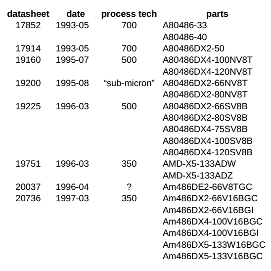
Packaging reveals Process Technology?
There are 2 types of packaging, 168CPGA for desktops and 208SQFP for embedded applications.
The SQFP processor dies are buried in plastic, so no visible evidence of die size.
The PGA processors have a metal die cover on the pin side (back). There are 2 sizes of die cover, 18 mm x 18 mm and 20.5 mm x 20.5 mm.
I think:
20 mm die cover = die made with 700 nm process tech
18 mm die cover = die made with 500 nm or 350 nm process tech
AMD has used many different packages for PGA processors, and each type is numbered. The packages are numbered sequentially in time, thus lower package numbers correspond to earlier manufacturing runs, and higher numbers are later. Each package was used for various similar parts, so they are not useful for exact part identification. However, each package should be one particular physical implementation, so that different sized dies should never have the same package number.
I looked at AMD 486 CPUs in my collection, and online photo collections to determine die cover sizes for 8 different packages known for 486 PGA CPUs. There is good correlation. If the above is true, then:
20 mm die cover = 700 nm process tech in packages
24361
25220
<EDIT: This is edited, based on discussion below>
20 mm die cover = 500 nm process tech in package
25372
<end of EDIT>
18 mm die cover = 500 nm process tech in packages
25253
25255
25398
25498
18 mm die cover = 350 nm process tech in package
25544
Package 25372 - what process tech?
The oddity in this list is package 25372. The number 25372 suggests that manufacture started after 500 nm process tech was in use, but it has the larger 20 mm die cover used by earlier packages. I found only 3 photos of CPUs with package 25372, so it is uncommon. Look at these 3 CPUs:
1. revision B date 9538 part A80486DX4-100SV16B http://cdn.cpu-world.com/Images/uploaded/0000/81/L_00008199.jpg
2. revision B date 9539 part A80486DX4-100SV16B http://www.cpu-info.com/img/cpu/80486/AMDA80486DX4-100SV16B-L.jpg
3. revision C date 9646 part A80486DX4-100SV8B http://abload.de/img/tmp_9268-2015-05-27_2fhq61.jpg
The first 2 of these have part numbers that indicate 16 KB L1 cache. This seems incredible because AMD datasheets start mention of 16 KB cache CPU only when they began 350 nm process tech. All of the 16 KB cache CPUs except these have package 25544, indicating 350 nm process tech. The earliest package 25544 that I have seen has date code 9551.
(Compare datasheet 19225 "Enhanced Am486® Microprocessor Family" (pdf) from March 1996 to datasheet 20736 "Enhanced Am486®DX Microprocessor Family" (pdf) from March 1997.)
Have you seen other 16 KB cache 486 with package number other than 25544?
Are these 2 CPU real or fake?
Is it possible to have 16 KB cache on a 700 nm process?
What process tech is used on the dies in package 25372?
Last edited by Neon on Sat Jun 06, 2015 8:21 am; edited 1 time in total |
|
| Back to top |
|
 |
Birdman.

Joined: 13 Nov 2012
Posts: 833
Location: Finland
|
| Posted: Fri Jun 05, 2015 3:08 am Post subject: |
|
|
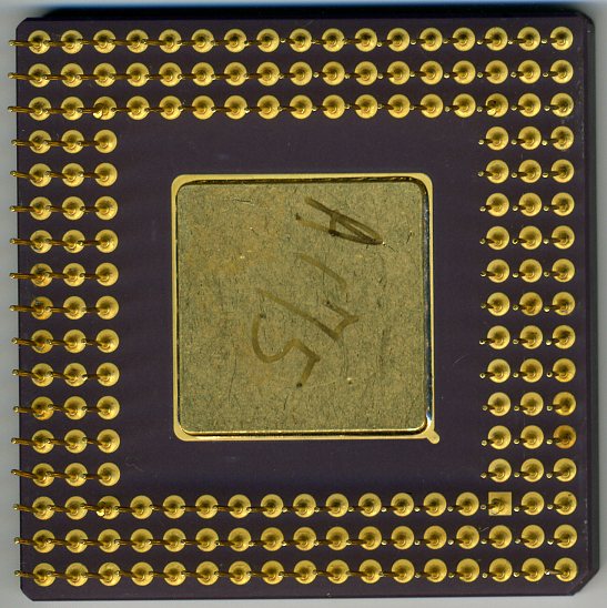
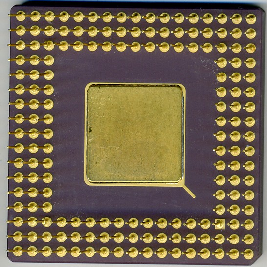
At least a die with 16 KB cache is significantly longer than a die with 8 KB cache, so likely 16 KB at 700 nm wouldn't fit even under larger lid, so it could be 16 KB at 500 nm instead. It's also possible that lid is just oversized without larger die than usually.
You can see the size difference between 8 KB and 16 KB in my die shots:
A80486DX4-120SV8B:

AMD-X5-133ADW:
 |
|
| Back to top |
|
|
Neon
Joined: 04 Feb 2008
Posts: 1512
Location: Dallas, Texas, USA
|
| Posted: Fri Jun 05, 2015 9:53 am Post subject: |
|
|
Ooh, big size difference.
Yes, I think it makes sense that package 25372 contains a die that was early 500 nm process technology with 16 KB cache.
Perhaps manufacturing yield was low, which would explain why there are few 25372 packages. Then, 16 KB cache would wait until 350 nm process was ready. |
|
| Back to top |
|
|
CPUShack

Joined: 16 Jun 2003
Posts: 34259
Location: State of Jefferson, USA
|
| Posted: Fri Jun 05, 2015 11:54 am Post subject: |
|
|
the 16K die could have been used for 8KB chips too, and if yields were low, is very likely to have been used as such.
Disable the bad block(s) of cache, and sell as an 8KB
_________________
New for 2025! The CPU Shack has a co-processor!
Visit The CPU Shack of microprocessor history and information. |
|
| Back to top |
|
|
frag_
Joined: 17 Nov 2008
Posts: 4015
Location: Estonia
|
| Posted: Sat Jun 06, 2015 12:06 pm Post subject: |
|
|
Very interesting research, thank you!
>20 mm die cover = 700 nm process tech in packages
>24361
>25220
Then some DX2-66 (24361 and 25220 packages) and even DX2-80 (25220)
should be 700 nm too? |
|
| Back to top |
|
|
Neon
Joined: 04 Feb 2008
Posts: 1512
Location: Dallas, Texas, USA
|
| Posted: Sat Jun 06, 2015 1:09 pm Post subject: |
|
|
| frag_ wrote: | Very interesting research, thank you!
>20 mm die cover = 700 nm process tech in packages
>24361
>25220
Then some DX2-66 (24361 and 25220 packages) and even DX2-80 (25220)
should be 700 nm too? |
Yes, I believe this is correct, but I do not know.
It would be helpful if AMD supplied this information.
I plan to continue to collect data, and seek fuller explanation. |
|
| Back to top |
|
|
Birdman.
Joined: 13 Nov 2012
Posts: 833
Location: Finland
|
| Posted: Sat Jun 06, 2015 4:31 pm Post subject: |
|
|
| Check chip33 at http://www.pbase.com/fotoopa/inside. That's A80486DX2-80NV8T with larger lid, 25220 package and 700 nm die. I should get similar one for die shot soon. |
|
| Back to top |
|
|
CPUShack
Joined: 16 Jun 2003
Posts: 34259
Location: State of Jefferson, USA
|
|
| Back to top |
|
|
Neon
Joined: 04 Feb 2008
Posts: 1512
Location: Dallas, Texas, USA
|
| Posted: Sun Jun 07, 2015 4:51 pm Post subject: |
|
|
CPUShack,
Yes, probably. If you look at the revisions, it suggests that the transition from 700 nm to 500 nm process took place during package 25220.Transition from 500 nm to 350 nm process took place during package 25498. So, it gets a little complicated.
I have started a table with timeline information to show this, but the data is limited to what I have observed so far.
Last edited by Neon on Mon Jun 08, 2015 7:23 pm; edited 1 time in total |
|
| Back to top |
|
|
diodenmann

Joined: 07 Apr 2008
Posts: 69
|
| Posted: Mon Jun 08, 2015 2:23 pm Post subject: |
|
|
I browsed through my collection and found some additional model data you can add to your list:
25220 A 9448 DX2-80 V8T
25220 A 9449 DX2-66 V8T
25253 AY 9506 DX4-100 NV8T
25255 B 9526 DX4-100 SV8T
25398 C 9604 DX4-120 SV8B
25498 C 9620 DX4-100 SV8B
25498 C 9623 DX4-100 SV8B
25498 CV 9622 DX4-100 SV8B
25544 A 9549 X5-133 ADY |
|
| Back to top |
|
|
CPUShack
Joined: 16 Jun 2003
Posts: 34259
Location: State of Jefferson, USA
|
|
| Back to top |
|
|
Neon
Joined: 04 Feb 2008
Posts: 1512
Location: Dallas, Texas, USA
|
| Posted: Mon Jun 08, 2015 7:23 pm Post subject: |
|
|
Thank you for additional data. I have included it in my timeline table.
Last edited by Neon on Tue Jun 09, 2015 11:55 pm; edited 1 time in total |
|
| Back to top |
|
|
Birdman.
Joined: 13 Nov 2012
Posts: 833
Location: Finland
|
| Posted: Mon Jun 08, 2015 10:00 pm Post subject: |
|
|
| Shouldn't 25220 rev A be still 700 nm? At least opened chip33 at http://www.pbase.com/fotoopa/inside clearly has larger 700 nm die. |
|
| Back to top |
|
|
CPUShack
Joined: 16 Jun 2003
Posts: 34259
Location: State of Jefferson, USA
|
|
| Back to top |
|
|
frag_
Joined: 17 Nov 2008
Posts: 4015
Location: Estonia
|
|
| Back to top |
|
|
|

