| View previous topic :: View next topic |
| Author |
Message |
Katmai500

Joined: 30 Sep 2010
Posts: 360
Location: Southern NJ, USA
|
 Posted: Wed Jul 03, 2019 9:59 am Post subject: The Pentium Pro: 0.5 or 0.6 µm? + cache combinations Posted: Wed Jul 03, 2019 9:59 am Post subject: The Pentium Pro: 0.5 or 0.6 µm? + cache combinations |
 |
|
This started off as a simple observation that turned into a two hour rabbit hole of determining if the Pentium Pro was built on the 0.5 µm or 0.6 µm process node.
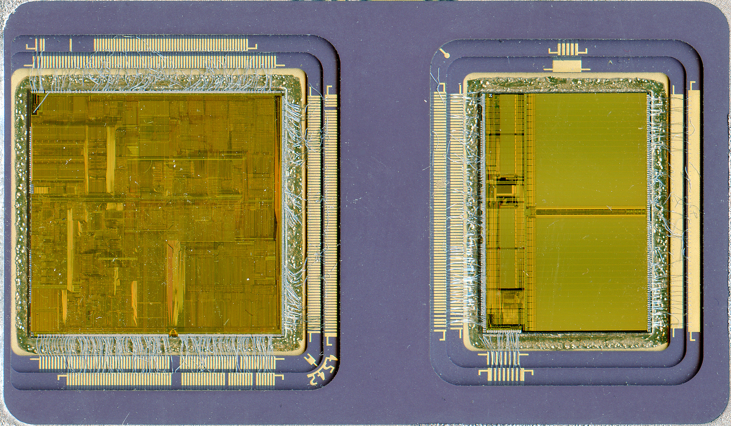
I was reading xsecret's post about his Intel KJ8TSMR00-BA ES, and the speculation about what it is. Then I was looking at the die shot of the Pentium Pro cache test chip posted by CPUShack to confirm for myself that it was an early 512K Pentium Pro cache die, which seems plausible when looking at a side-by-side comparison.
Then I started comparing photos of de-lidded Pentium Pro CPUs and trying to figure out all the combinations of process nodes and cache sizes that were produced. Looking at the CPU-World database, I see it listed as 0.6 µm (P652) and 0.35 µm (P854). I did some more digging and saw that the Pentium Pro Wikipedia article claims the following:
| Quote: | The 133 MHz Pentium Pro prototype processor die was fabricated in a 0.6 µm BiCMOS process.[15][16]
The 150 MHz Pentium Pro processor die was fabricated in a 0.50 µm BiCMOS process.[16][17]
The 166, 180, and 200 MHz Pentium Pro processor die was fabricated in a 0.35 µm BiCMOS process.[16][17]
The 256 KiB L2 cache die was fabricated in a 0.50 µm BiCMOS process.[16][17]
The 512 and 1024 KiB L2 cache die was fabricated in a 0.35 µm BiCMOS process.[16][17] |
The Wikipedia List of Pentium Pro microprocessors matches.
| Quote: | The 150 MHz Pentium Pro processor dies (B0, C0) used a 0.50 μm BiCMOS process.
The 166, 180, and 200 MHz Pentium Pro processor dies (sA0, sA1, sB1) used a 0.35 μm CMOS process.
The sA0 stepping is logically equivalent to the C0 stepping, but on a different manufacturing process.[1]
The 256 KB L2 cache dies (256/α, 256/β) used a 0.50 μm BiCMOS process.
The 512 KB and 1 MB L2 cache dies (512/α, 512/β, 1024/γ) used a 0.35 μm CMOS process. |
However, the one source they cite that I could find indicates that the 150 Mhz production CPU was produced in 0.6 µm, not 0.5 µm. (Tuning Pentium Pro Microarchitecture - IEEE Micro). This is also backed up by an archived intel webpage regarding the Pentium Pro. The intel page also states that the 256K cache die was 0.6 µm.
However, this edition of the Microprocessor Report claims that the 150 Mhz production CPU and 256K cache dies were both 0.5 µm.
I can't find any definitive die shots of an early Pentium Pro sample to compare the die to the production 150 Mhz die. I'm curious if anyone here has any solid data on this 0.6 µm vs 0.5 µm discussion. The process nodes are fairly close together, so maybe intel used the terms interchangeably? The Pentium appears to have skipped the 0.5 µm node entirely, jumping from 0.6 µm for the 100 Mhz model to 0.35 µm for the 120+ Mhz models.
As far as the CPU die and cache combinations, it seems pretty straightforward for the production CPUs:
- 150 MHz -> 0.6/0.5 µm CPU + 0.5 µm 256K cache
- 166 MHz -> 0.35 µm CPU + 0.35 µm 512K cache
- 180 MHz -> 0.35 µm CPU + 0.5 µm 256K cache
- 200 MHz -> 0.35 µm CPU + 0.5 µm 256K cache
- 200 MHz -> 0.35 µm CPU + 0.35 µm 512K cache
- 200 MHz -> 0.35 µm CPU + 0.35 µm 512K cache + 0.35 µm 512K cache
|
|
| Back to top |
|
 |
xsecret

Joined: 01 Feb 2004
Posts: 1847
Location: France
|
| Posted: Wed Jul 03, 2019 11:14 am Post subject: |
|
|
P652 (0.6µm) process and P852 (0.5 µm) are very similar. Gate oxide thickness is identical on both. The major difference being the size of the wafer (6" vs 8"). It's easy to switch from P652 to P852 (but much more difficult to switch from P852 to P854, 0.35µm).
This said, P852 was ready by the end of 1993 and the first known samples of the P6 are from 1995. It makes no sense for Intel to tape-out an A0 spec on P652 in 1995 (or even 1994).
I have an A0 P6 without lid. Wait a minute, I'll scan it...
_________________
ES-Only Collector : http://www.engineering-sample.com
Universal Chip Analyzer (UCA) : https://x86.fr/uca / http://www.cpu-world.com/forum/viewtopic.php?t=34349 |
|
| Back to top |
|
|
xsecret
Joined: 01 Feb 2004
Posts: 1847
Location: France
|
|
| Back to top |
|
|
xsecret
Joined: 01 Feb 2004
Posts: 1847
Location: France
|
| Posted: Wed Jul 03, 2019 12:34 pm Post subject: |
|
|
About the KJ8TSMR00-BA, everyone (including me) thought it's related to the Pentium Pro because its huge ceramic packaging.
But when you have the actual chip in hand, you notice the size is MUCH smaller. Not bigger than a 486.
I scanned everything and put all the dies to the same scale, then measured them all. Check that :
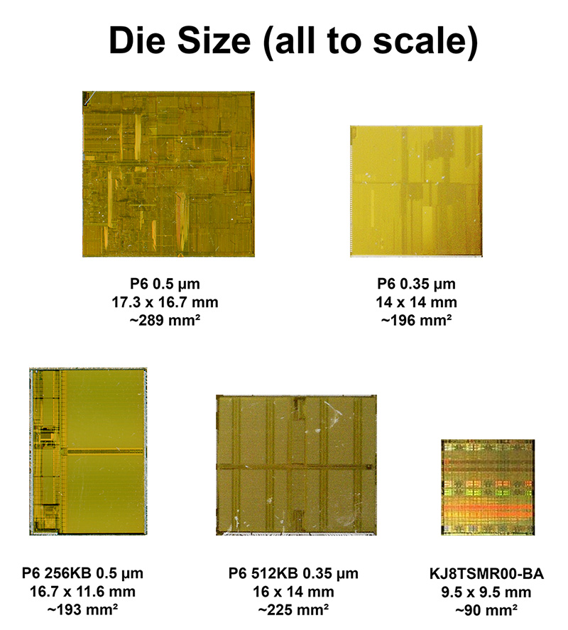
The KJ8TSMR00-BA die (almost sure built on 0.35 µm) is way too small for anything related to P6. :-/
_________________
ES-Only Collector : http://www.engineering-sample.com
Universal Chip Analyzer (UCA) : https://x86.fr/uca / http://www.cpu-world.com/forum/viewtopic.php?t=34349 |
|
| Back to top |
|
|
bccwchan

Joined: 20 Sep 2004
Posts: 2585
Location: Hong Kong
|
| Posted: Wed Jul 03, 2019 8:35 pm Post subject: |
|
|
I still believe the A8CNIC is the cpu and the KJ8TSMR00-BA is the cache produced for testing purpoase.
Please refer to the old thread about the unknown ES A8CNIC.
http://www.cpu-world.com/forum/viewtopic.php?t=7877&postdays=0&postorder=asc&highlight=a8cnic&start=30
If you claim that the A8CNIC is the cpu then Intel should have the cache for the cpu.
I claim the KJ8TSMR00-BA because the production of the A8CNIC and KJ8TSMR00-BA are quite similar. One is week 23 year 1996 and another one is week 17 year 1996. |
|
| Back to top |
|
|
bccwchan
Joined: 20 Sep 2004
Posts: 2585
Location: Hong Kong
|
| Posted: Wed Jul 03, 2019 8:48 pm Post subject: |
|
|
| I bought two ES in 2013 from ebay. It clearly showed that Intel used the PPro cache for some testing. |
|
| Back to top |
|
|
xsecret
Joined: 01 Feb 2004
Posts: 1847
Location: France
|
| Posted: Thu Jul 04, 2019 4:18 am Post subject: |
|
|
I don't claim A8CNIC is the CPU because I don't know and I don't have one. But I have a KJ8TSMR00-BA and we have only speculations about its relation with P6. But it makes not sense for Intel to build a special costly "test CPU" in Q2'1996 for the P6 µarch because they already had working samples for it. More, at that date, they works on Klamath. P6 was finished long before.
Fact about KJ8TSMR00-BA is the die inside is way too small to be 512 or even 256 KB of cache. The pattern also doesn't match, with too much logic and too few SRAM cells. It seems to be a small cache (64/128 KB) with a high speed bus. Like the one needed for RAID controllers or NIC.
PS: Your last picture deserves a better scan 
_________________
ES-Only Collector : http://www.engineering-sample.com
Universal Chip Analyzer (UCA) : https://x86.fr/uca / http://www.cpu-world.com/forum/viewtopic.php?t=34349 |
|
| Back to top |
|
|
bccwchan
Joined: 20 Sep 2004
Posts: 2585
Location: Hong Kong
|
| Posted: Thu Jul 04, 2019 9:25 am Post subject: |
|
|
| Same 256k cache was used in PPro and the Pentium-like cpu. I therefore believe Intel have done the same testing on the PII cpu. |
|
| Back to top |
|
|
xsecret
Joined: 01 Feb 2004
Posts: 1847
Location: France
|
| Posted: Thu Jul 04, 2019 10:33 am Post subject: |
|
|
A 256 KB cache built on 0.35 µm would require ~135 mm² of die space. The KJ8TSMR00-BA die is only 90 mm². So it's impossible to have more than 128 KB of SRAM inside.
This said, Klamath uses 4x 128 KB chips, but these IC were outsourced to Toshiba or NEC. And they have much less pins.
Maybe these IC are related to some kind of supercomputer. :-/
PS : With the last picture you posted, there is no doubt that your IC is an external Pentium Pro cache IC. Pity there is no date code, but it's probably much older than KJ8TSMR00-BA :-/
_________________
ES-Only Collector : http://www.engineering-sample.com
Universal Chip Analyzer (UCA) : https://x86.fr/uca / http://www.cpu-world.com/forum/viewtopic.php?t=34349 |
|
| Back to top |
|
|
Katmai500
Joined: 30 Sep 2010
Posts: 360
Location: Southern NJ, USA
|
| Posted: Mon Jul 08, 2019 9:58 pm Post subject: |
|
|
AWESOME discussion going on in here, and thanks xsecret for the really detailed follow-up! 
I figured it wouldn't make sense for intel to use P652 for even the earliest Pentium Pro samples, given the date codes, but kept seeing those references to 0.6 µm. The fact that P652 and P852 share the same gate oxide thickness probably explains the mixed use of the terms in period articles.
I didn't take the time to put mine to scale. Doing so like you did definitely proves that the KJ8TSMR00-BA ES isn't a 512K Pentium Pro cache. A 128K 0.35 µm cache seems plausible, but what would have been the purpose?
bccwchan, that 256K cache die in the Pentium-like package is really cool. All these unique test packages are really interesting. |
|
| Back to top |
|
|
|