| View previous topic :: View next topic |
| Author |
Message |
xsecret

Joined: 01 Feb 2004
Posts: 1847
Location: France
|
 Posted: Mon Dec 18, 2017 9:28 am Post subject: Introducing the U.C.A - Upd #15 (Final DIP40 Adapter) Posted: Mon Dec 18, 2017 9:28 am Post subject: Introducing the U.C.A - Upd #15 (Final DIP40 Adapter) |
 |
|
Updates
- 2017-12-20 : Added support for MCS-51 (iAPX86 UCAS)
- 2017-12-22 : Added support for MCS-48 (iAPX86 UCAS)
- 2017-12-31 : Added support for Z80 (iAPX86 UCAS)
- 2018-01-31 : Added support for NSC800 (iAPX86 UCAS)
- 2018-02-08 : Tethered Mode implemented for advanced analysis & benchmark mode.
- 2018-02-11 : Added support for RCA 1802/COSMAC (iAPX86 UCAS)
- 2018-04-24 : Added support for Signetics 2650 (iAPX86 UCAS)
- 2018-07-30 : Added support for Intel 8080 (iAPX86 UCAS)
- 2019-03-25 : Added support for MOS 6502 (iAPX86 UCAS)
- 2019-07-16 : Added support for Motorola 6800 (iAPX86 UCAS)
- 2024-01-15 : Final UCA Announced
- 2024-09-09 : Added support for (EE)PROM
- 2024-10-06 : Added support for Intel 8008
- 2024-12-10 : Major Upgrade for the final DIP40 Adapter!
I'm so excited to finally disclose my project here for the first time. I know that only few people may have any interest in this kind of stuff, but as fellow collectors, you're certainly in those ones. The idea came to my mind last summer, when I read one of the amazing announcement from molka. I realized that, even if I have some skills in electronics and product design, I don't have any clues about how earliest CPUs worked back in the 70s & 80s. So, I started to study one of the most successful architecture from that era, the Intel 8086. After some basic experimentation on a breadboard, I then started thinking about an ambitious "universal" IC tester and how to build it.
The Ideal Specs
Ideally, I wanted the specification to be as such:
- Versatile: Able to check the working condition of many different ICs. As much as possible. CPUs, of course, but also other kind of chips like microcontrollers, BSPs, RAMs, and why not FPUs or other support chips. Sounds like crazy because all these ICs are totally different beasts from an electrical interface point of view. Even a 8086 is vastly different from a 8085.
- Advanced: With two testing modes. One basic testing mode, that only requires the UCA and a standard USB power bank to provide the 5V required. You get the result on built-in LEDs. And also one more advanced "analyzer" mode, with the UCA tethered to a computer with USB. With an app, you can get some additional information like real-time power composition, chip identification, working condition, and maybe TBD stuff, depending of the kind of IC tested. On top of that, I also wanted to have "advanced" features. I.e.: testing the working condition of an IC is nice, but testing it at its rated clock frequency is even better. What about overclocking? Benchmark? Could be great too.
- Secure: I'm a CPU collector and I don't want to burn a costly ES if something goes wrong. The UCA need to be able to detect short-circuit or other defaults. Safety first!
- Compact: I didn't want a bulky tester. I tried to keep it as small as possible. The actual footprint (8x6 cm) is barely bigger than a credit card.
- Upgradable: Most of the "intelligence" must be in software. The upgradability of the UCA was mandatory. I wanted to be able to upgrade the firmware via USB, to add support for new chips without any (or too much) hardware modifications. More interesting, I also wanted to let the user write his OWN code for the target CPU. So, the UCA can act as a development board.
- Future-proof: When I started my first experiments with the 8088, I had to buy and mess around with Intel 8284 clock generator, bus controllers and other support chips. Some of them aren't manufactured anymore since decades, are hard-to-find and/or expensive. I wanted to get rid of ANY obsolete chips and I'm only using modern ICs widely available.
- Cheap: From a technical view, everything I described is close to a device I already own, the Galep-5 Universal EEPROM programmer. It's a very nice piece of hardware but it costs more than 500� (and that's without the numerous expensive adapters often required). I'm not exactly a rich man so I had to keep the price as low as possible. The U.C.A. doesn't use fancy components. The total BOM is lower than $50. Of course, the final price also depends on manufacturing costs. The fewer I order, the higher the price will be.
So here we are. From all the crazy specs described previously, only a few are working right now. I'm not pretentious enough to tell that all of them will work one day, but the current progress seems to prove the whole project isn't a total failure. A pretty good start! 
How It Is Built
Let's talk about the UCA. The most obvious central component to use is an FPGA. Microcontrollers are just too slow to interface at full speed with even a 8086 from the 80s, and I have more ambitious target CPU in mind. FPGAs have a lot of IO pins and can be software reconfigurable to accommodate a variety of pinouts. They're also extremely fast. Main issue (at least for me): developing FPGA and writing HDL code is a nightmare. We're clearly not in the same world as Arduino or Raspberry Pi.
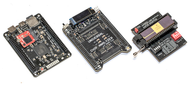
Developing a compact FPGA PCB with 100+ I/O is not extremely complex, but it's not cheap. You must use a 4-layer PCB (or more) and solder a fine-pitched QFP or BGA IC. In small quantities, the price skyrockets very quickly. So, I looked at the FPGA development boards already available in the market. No need to reinvent the wheel if something suitable was already created and mass-produced. All the UCA's intelligence is inside the HDL code that emulates (almost) everything and doesn't require fancy electronics. I found the perfect board: The Mojo from Embedded Micro. It was a successful Kickstarter project launched in 2013 that raised more than $100k.
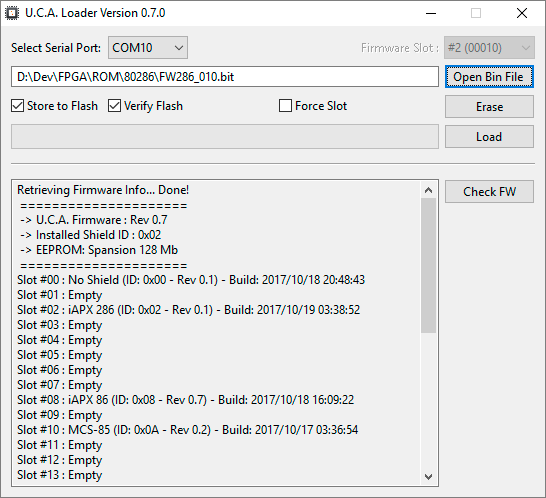
The Mojo is a simple board packed with an Atmel ATMEGA 32U4 microcontroller, 4 Mb Flash EEPROM and a Xilinx Spartan 6 FPGA. To fit my needs, I modified the original Mojo to add 128 Mb of EEPROM Flash and a stronger voltage regulation. That only requires swapping some components but doesn't need any PCB modifications, so I was able to keep the original PCB layout. Of course, the original Mojo firmware burnt into the ATMega32U4 had to be rewritten, as well as the original FPGA firmware upload tool.
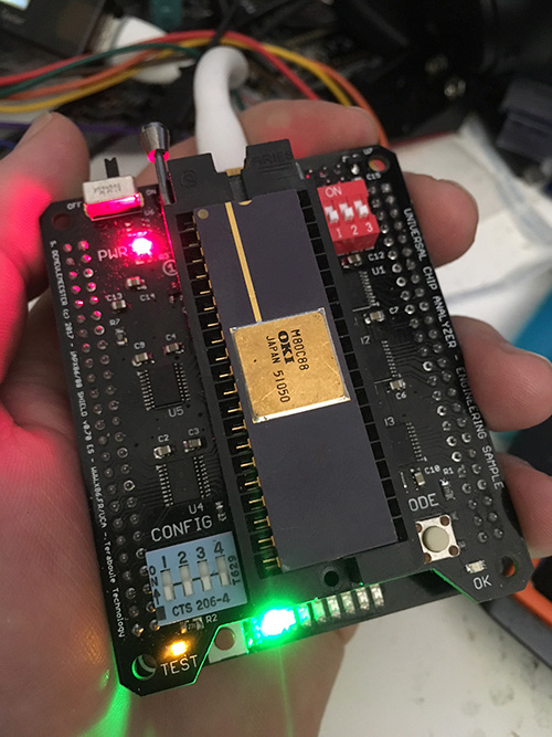
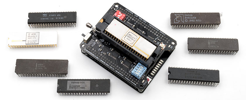
We now have the UCA itself. Then we need an interface to old chips. Modern FPGAs require 3.3V while most IC introduced before mid-90 use 5V (or much higher voltages for the pre-TTL era). The idea here is to use another PCB plugged on top of the UCA (called "UCA Shield" or UCAS). The UCAS is a low-cost, removable PCB. It can be switched to another one to support other IC family. Some UCAS can support many different chips, just by setting a DIP switches. Some chips works without any other modification, just by plugging them into the ZIF Socket, some will require a (very) cheap adapter on top to accommodate different packages (PLCC, LCC, etc.) or different power pinouts.
Current State
About the UCA, I successfully modified the original Mojo hardware. The firmware has been rewritten to work with the new EEPROM, supports many different FPGA configuration slots (up to 32 right now). I also added many tweaks (automatic detection for shield swap/DIP setting change, A/D converter modification, etc.). The firmware update tool has also been adapted for the UCA. There is still some work required, but the platform is quite stable right now. The whole process of building/uploading/loading FPGA configuration on multiples slot is almost done. Right now, I didn't start working on the "tethered" part. I added some functions on the UCA firmware, but the Windows part has yet to be done.
About the UCA Shields (UCAS), the whole project started with the iAPX 86 UCAS. The current revision for that Shield is 0.7 and all the most important hardware parts are working as expected. After 3 months of intensive testing, I found some additional tweaks that must be added. Most of them are dedicated to ease the support for some IC. One (maybe two) revisions of the PCB will be required before the "final" one.
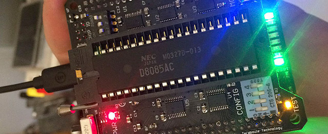
Right now, the iAPX 86 UCAS is able to fully test all 8088 and 8086. Clock frequency can be set to 4 MHz (slowest commercially available freq), 8 MHz (8086-2), 10 MHz (8086-1) and 12.5 MHz (overclocking or some Harris parts). 8088s are tested using a 8-bit interface, 8086s with a 16-bit data bus (autodetected). NEC V20/V30 are of course also supported (and detected with the DIAG button). 8018x will require a UCAS Adapter because they use a different Socket. I didn't start working on this one, but it's pretty trivial. To validate the concept of complete reconfiguration, I worked on support for 8085 on the iAPX 86 UCAS. All 8085s can now be fully tested just with a different DIP Switch setting. I'm now working on other type of IC (MCS-51, Z80, etc.). Right now, I can't guarantee any of them will work, but I'm confident they will.
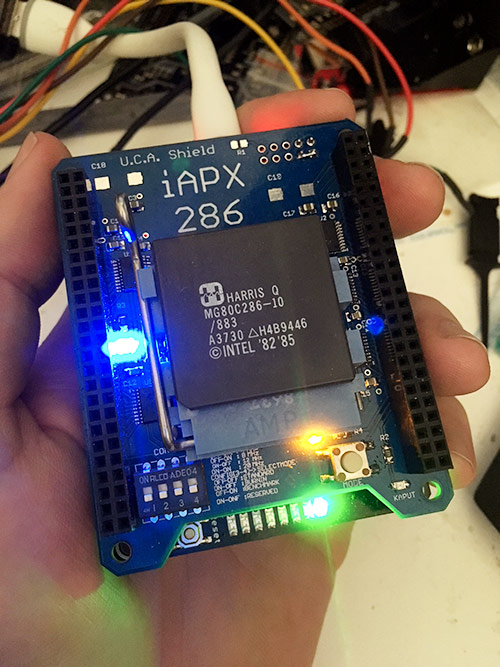
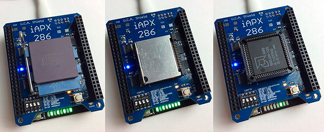
As a proof-of-concept and to demonstrate the power of the FPGA-powered UCA, I also worked on a iAPX 286 UCAS. The revision 0.1 is done and works as expected. It can test any 80286 in PGA/PLCC/LCC. It still lacks almost all advanced features and need a lot of optimization, but it's only a matter of time. A 386 UCAS is also possible after this one, and perhaps also a 486 UCAS. The main issue is the space required by the ZIF Socket. But I still have a LOT of work before thinking at 386 and newer CPUs�
Some other UCAS are also in the pipe (4004/4040/8008/8080, RAM UCAS, etc.) but I really need to finalize the current shields before starting other ones. That will be a LONG process, probably spread on several years.
Want to Know More?
There is still gazillions of details I would love to share, but I've crossed the TL;DR line since a very long time. For the few of you that want to know more, I just started a website describing the project further. It's far from being finished but you can probably grab some more information there.
UCA website is here: https://x86.fr/uca/
You can see it in action here : https://www.youtube.com/watch?v=ic-VPV17CHI
Some additional pictures :
More pictures coming soon... You can also have a look at the "Compatibility" tab 
Feedbacks needed!
I need your thoughts! Currently, I have no idea about the level of interest for this project. I didn't start this to make big money. I've already learn a lot of things about FPGAs and old chips and I'm sure I still have a lot to learn in the future. It's enough to keep me happy. However, I already have some contacts to produce both the UCA and the UCAS if required. Hand soldering is not really an option for more than 2-3 pcs (I need 3 hours to assemble just one board).
Whether or not you're interested in having one, I'll greatly appreciate if you can share your thoughts. Things will be different if only 2-3 fellow collectors cares about the UCA, or if there is more demand. What's the next IC family to focus on? What features would you like me to add? Do you see any major drawbacks? You can also give me your opinion about the "best" price (will tell you more on that if somebody cares).
Of course, I'll be glad to answer any questions you may have! I'll post the updates about UCA and UCAS on this thread, and some additional pictures soon.
PS: Thanks to John for his invaluable help in the first stages of this project. I know I bothered him a lot with tons of silly questions.
_________________
ES-Only Collector : http://www.engineering-sample.com
Universal Chip Analyzer (UCA) : https://x86.fr/uca / http://www.cpu-world.com/forum/viewtopic.php?t=34349
Last edited by xsecret on Mon Dec 09, 2024 7:39 pm; edited 23 times in total |
|
| Back to top |
|
 |
alexzu
Joined: 12 May 2016
Posts: 272
|
| Posted: Mon Dec 18, 2017 9:55 am Post subject: |
|
|
| Looks like tons of work .. great job ! ) |
|
| Back to top |
|
|
Vegeta

Joined: 13 Apr 2013
Posts: 7049
|
| Posted: Mon Dec 18, 2017 10:02 am Post subject: |
|
|
Very nice!
_________________
Wanted: 4 x VT-25-A tubes |
|
| Back to top |
|
|
CPUShack

Joined: 16 Jun 2003
Posts: 34259
Location: State of Jefferson, USA
|
|
| Back to top |
|
|
max1024

Joined: 15 Jan 2015
Posts: 636
Location: Belarus
|
| Posted: Mon Dec 18, 2017 1:02 pm Post subject: |
|
|
| I see that a huge amount of work has been done! I like people who invent something new and generally understand the intricacies of old HW. I wish you success in your development and that your enthusiasm is not exhausted. It's a great Project Good luck! |
|
| Back to top |
|
|
xsecret
Joined: 01 Feb 2004
Posts: 1847
Location: France
|
|
| Back to top |
|
|
D.8080

Joined: 03 Apr 2006
Posts: 1474
Location: Italy
|
| Posted: Mon Dec 18, 2017 1:17 pm Post subject: |
|
|
| You made my day. |
|
| Back to top |
|
|
max1024
Joined: 15 Jan 2015
Posts: 636
Location: Belarus
|
| Posted: Mon Dec 18, 2017 1:46 pm Post subject: |
|
|
| I write more. I know people who make big projects, but at the exit we have ugly and unpleasant things. As Steve Jobs sad: the design should be perfect! I like non-standard laconic industrial design, and in your project everything is perfect I think, It is the pleasure to looking on this working sample ))) |
|
| Back to top |
|
|
xsecret
Joined: 01 Feb 2004
Posts: 1847
Location: France
|
| Posted: Mon Dec 18, 2017 1:59 pm Post subject: |
|
|
Yes! It's tempting to add more and more features, but a lot of them are almost useless. When I started designing the iAPX86 Shield, I messed with small OLED display and other fancy things like that. But I realized this will add a lot a complexity to the design, boost the price significantly, without adding anything really useful. The heart of this project is the HDL implementation of all the support chips required (including RAM & ROM). I'll keep focusing on that.
_________________
ES-Only Collector : http://www.engineering-sample.com
Universal Chip Analyzer (UCA) : https://x86.fr/uca / http://www.cpu-world.com/forum/viewtopic.php?t=34349 |
|
| Back to top |
|
|
max1024
Joined: 15 Jan 2015
Posts: 636
Location: Belarus
|
| Posted: Mon Dec 18, 2017 2:21 pm Post subject: |
|
|
| Unfortunately, I do not know all the information of testing processors and what mechanisms occur during testing. But the idea with the LED display is quite the place to be. For those users who do not understand until the end of the mechanism and result of testing, the display can display understandable information, but I think this greatly complicates the development and will require a lot of time and money too. |
|
| Back to top |
|
|
xsecret
Joined: 01 Feb 2004
Posts: 1847
Location: France
|
| Posted: Mon Dec 18, 2017 2:33 pm Post subject: |
|
|
Exactly. That's why I added the two modes : the standalone mode uses LEDs to display the test partern and the DIAG button to display a binary code corresponding to the detected features (8- or 16- bit data bus, V20/V30, etc.). It's extremely simple and easy to use for everyone. Basically, you just have to configure the DIP switch for the target family, put the IC into the Socket than flip the ON/OFF switch.
For more advanced testing, much more information will be available when the UCA is tethered to a computer via USB.
_________________
ES-Only Collector : http://www.engineering-sample.com
Universal Chip Analyzer (UCA) : https://x86.fr/uca / http://www.cpu-world.com/forum/viewtopic.php?t=34349 |
|
| Back to top |
|
|
xsecret
Joined: 01 Feb 2004
Posts: 1847
Location: France
|
|
| Back to top |
|
|
aduream

Joined: 30 Apr 2012
Posts: 445
Location: beijing china
|
| Posted: Mon Dec 18, 2017 7:41 pm Post subject: |
|
|
| Strong support for you |
|
| Back to top |
|
|
xsecret
Joined: 01 Feb 2004
Posts: 1847
Location: France
|
| Posted: Tue Dec 19, 2017 11:55 am Post subject: |
|
|
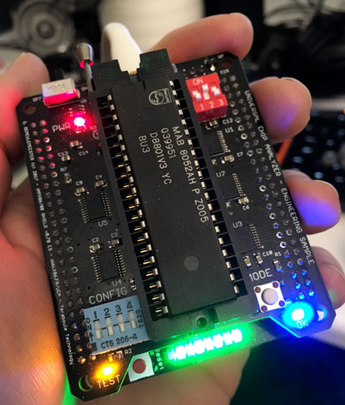
The first steps for supporting the very common MCS-51 microcontrolers are done. And it works, just with a firmware update and without any hardware mod on the iAPX86 UCAS !
Right now only at 8 MHz because of timings issues in the early HDL code, but I'm working on it right now. I've ordered a supercharged modern MCS-51 IC. Hope to have more news tomorrow !
PS : The almost-final iAPX86 UCAS PCB (rev 0.9 "QS") is finished. I will order some pcs soon.
_________________
ES-Only Collector : http://www.engineering-sample.com
Universal Chip Analyzer (UCA) : https://x86.fr/uca / http://www.cpu-world.com/forum/viewtopic.php?t=34349 |
|
| Back to top |
|
|
molka

Joined: 17 Mar 2011
Posts: 2416
Location: Budapest, Hungary
|
| Posted: Tue Dec 19, 2017 4:24 pm Post subject: |
|
|
Incredibly impressive project. Very good idea and design. Congratulations!
Wish I had known about Mojo and what FPGA was. 
_________________
----------------------------------------------------------
My collection
http://www.x86-guide.net/molka/en/collection.html |
|
| Back to top |
|
|
|
|
|
|
|
You can post new topics in this forum
You can reply to topics in this forum
You cannot edit your posts in this forum
You cannot delete your posts in this forum
You cannot vote in polls in this forum
You cannot attach files in this forum
You cannot download files in this forum
|
|
Powered by phpBB © 2001 phpBB Group
|